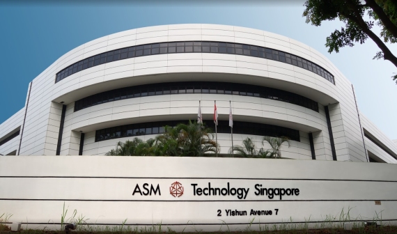
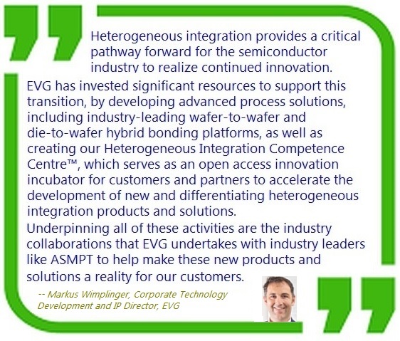
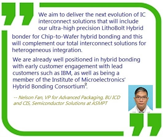
| Two global tech companies -- one headquartered in Singapore and the other in Austria -- have joined forces to create innovative solutions in the semiconductor space. ASM Pacific Technology and EV Group have signed an agreement to jointly develop die-to-wafer hybrid bonding solutions for 3D-IC/heterogeneous integration applications. lt is the industry's first such ultra precision bonding solutions, which will suit various applications, with optimal line balancing and process requirements, according to ASMPT's press release. ASMPT (HKEX stock code: 0522) is a leading global supplier of hardware and software solutions for the manufacture of semiconductors and electronics. It is run out of Singapore by Singaporean CEO Robin Ng. EV Group is a leading supplier of equipment and process solutions for the manufacture of semiconductors, microelectromechanical systems (MEMS), compound semiconductors, power devices and nanotechnology devices.  Photo: Joey Ng/Google Maps Photo: Joey Ng/Google Maps |
|
ASMPT stock price |
HK$113.10 |
|
52-week range |
HK$66.5 – 133.80 |
|
Market cap |
HK$46.3 b |
|
PE (ttm) |
55.5 |
|
Dividend yield |
1.23% |
|
1-year return |
8.4% |
|
Shares outstanding |
410.8 m |
|
Source: Bloomberg |
|
Die-to-wafer hybrid bonding is a pivotal process for enabling the redesign of system-on-chip (SoC) devices to 3D stacked chips via chiplet technology.
This involves combining chips with different process nodes into advanced packaging systems that can power new applications such as 5G, high performance computing (HPC) and artificial intelligence (AI).
Heterogeneous integration is crucial to extending Moore’s Law and enabling future generations of devices with increasing levels of performance.
Hybrid bonding involving wafer-to-wafer as well as die-to-wafer integration is a necessary process step to support heterogeneous integration.
The challenge involved in die-to-wafer hybrid bonding is to push the boundaries and confluence of technologies to achieve high throughput and high yields for mass production adoption, by blending together ultra-high-precision bonding, ‘wafer fabrication’ die preparation and handling in a Class 1 environment1 , and hybrid and fusion bonding technologies into a fully seamless solution.
1 Refers to a cleanroom environment where there is no more than 1 particle of dust in a cubic foot of air.
To achieve such ultra-precision, highly configurable die-to-wafer bonding capabilities requires well-matched equipment partners from the wafer fab and assembly space to come together to deliver solutions for the next level of package scaling.
This is what this two companies jointly aim to achieve.
Both companies are leaders in their respective areas, with EVG’s die preparation technology and front-end cleanliness for die-to-wafer hybrid bonding, and ASMPT’s ultra-high precision bonding of extremely thin dies.
Mr. Wimplinger added: “Through this joint development agreement with ASMPT, which leverages our EVG320 D2W die preparation and activation system and a dedicated version of our GEMINI fusion bonding system specially configured for die-to-wafer bonding with ASMPT’s benchmark die bonding solutions, we can offer the industry a complete hybrid die-to-wafer bonding process flow to help speed the deployment of heterogeneous integration technologies.”
 2 The Institute of Microelectronics (IME) is a research institute of the Singapore Agency for Science, Technology and Research (A*STAR). Its missions is to strategically add value to Singapore's semiconductor industry. Key research areas are in Heterogeneous Integration, Systemin-Package, Sensor, Actuators and Microsystems, RF & mmWave, SiC/GaN-on-SiC Power Electronics, and MedTech. |
For more info, see press release here.


